
Job oriented Industrial Training Program with Experts
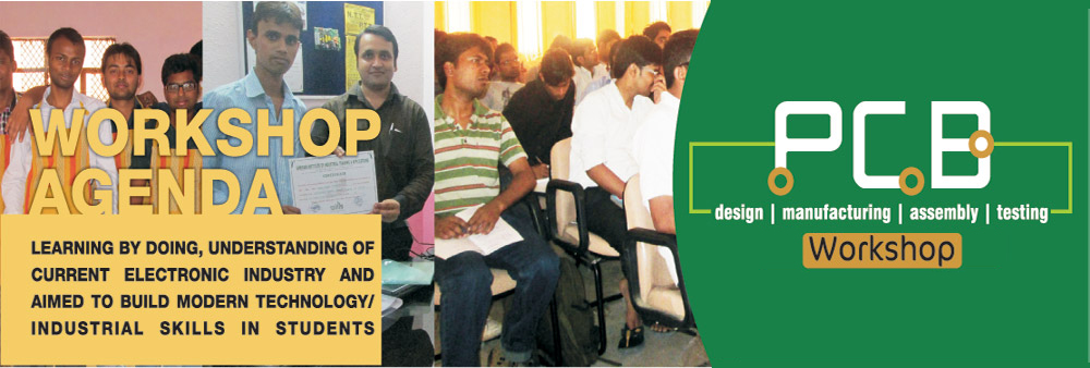
PCB Workshop Agenda Day1 | Day2 | Day3
TOPIC: Understanding PCB Design
• Introduction to PCB, Brief history
• Trends in PCB designing/ different type of PCB S/S, D/S, M/L
• Component identification
• Understanding the PCB design flow chat
• Understanding the schematic entry
• Creating library & components
• Preparing schematic
• Introduction to PCB layout
• Understanding units
• Component datasheet & foot prints creation
• Footprints library & browsing
• Starting PCB design
• Mechanical layer & mounting (size of PCB etc)
• Component placement
• Net list feeding
• Setting up rules
• Routing & editing
• DRC check
• Final o/p generation(Gerber, BOM, NC Drill file)
• O/p on butter paper & ideas for photo-plotting (+ve & -ve)
• Special focus on latest trends in PCB designing using SMDTOPIC: Competition for Best Activity
1st half of the day (Hands on session in PCB Designing)
• Mini projects by students on PCB designing on their own system. Minimum 1 or 2 activities in a day.
• Mini- project
• Power supply
• Multiivibrator
• BCD to decimal converter and many more2nd half of day (Hands on session in PCB Manufacturing)
• PCB fabrication of artwork designed by students
• Sheet cutting
• Film exposing
• Screen printing (ckt)
• Etching
• Drilling
• Masking
• Legend printing
• Tinning (roller)
• Final QC
• questions/ answers
• Certificate and prize distributionTOPIC: Assembly & Testing of Electronics Projects
• Distribution of PCBs & components for soldering
• Introduction to different types of soldering methods; (a) manual (b) dip (c) wave soldering
• Introduction to different testing equipments
• ESD protection
• Testing of loaded PCB for their running condition
• Q & A Session
• Certificate & prize distributionTo conduct a PCB Workshop at Institute or any other form of information regarding the PCB Workshop please contact on SIITA's HELP DESK NO.: +91 11 42420073 or mail at helpdesk@siita.co.in or drop down at Delhi office address.