 In today’s fast-growing electronics industry, PCB design has become one of the most sought-after skills. From smartphones and computers to IoT devices and automotive electronics, every device relies on a well-designed Printed Circuit Board (PCB). If you are looking to build a career in electronics, learning PCB design is no longer optional—it’s essential. But with so many courses available, how do you choose the right one? This guide will help you select the best pcb design course in Delhi that suits your career goals.
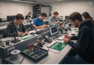
At Siita Institute, we offer comprehensive training programs that combine theoretical knowledge with hands-on experience, helping students become industry-ready professionals.
Why Learning PCB Design is Crucial
A PCB acts as the backbone of electronic devices, connecting components and ensuring proper functionality. Engineers who specialize in PCB design are in high demand across electronics manufacturing companies, startups, and research labs. Enrolling in a professional PCB manufacturing and design course in Laxmi Nagar provides you with the technical skills and practical knowledge required to succeed in this field.
Some benefits of learning PCB design include:
- Enhanced career opportunities in electronics and manufacturing companies.
- Ability to design and develop custom electronic circuits.
- Understanding of modern PCB manufacturing processes.
- Skill development that makes you industry-ready for placement.
Key Factors to Consider While Choosing a PCB Design Course
1. Comprehensive Curriculum
The first step in selecting the right course is checking the curriculum. A good course should cover:
- Basic electronics and circuit theory.
- PCB schematic and layout design.
- Multilayer PCB design techniques.
- Signal integrity, component placement, and routing.
- Fabrication process and PCB manufacturing standards.
At Siita Institute, our PCB Design course online with certificate in Laxmi Nagar includes all these topics with practical projects to ensure you gain in-depth knowledge.
2. Hands-On Practical Training
Theory alone is not enough in PCB design. Working on real PCB projects is essential to understand how concepts translate into real-world applications. Our pcb design course in Delhi emphasizes practical sessions where students design, fabricate, and test their own PCBs. This hands-on experience is invaluable for career growth.
3. Certification
A recognized certificate adds credibility to your skills. It not only boosts your resume but also helps you stand out to employers. Our PCB Design course online with certificate in Laxmi Nagar provides a certification recognized by top electronics companies, giving you an edge in interviews and job placements.
4. Placement Assistance
A course is truly valuable when it helps you land a job. Look for programs that offer placement support. Siita Institute is known for providing the Best PCB design course in Delhi with placement, helping students secure positions in reputable electronics firms after completing the course.
5. Learning Mode and Flexibility
With the growing demand for flexible learning, courses are now available both online and offline. Online courses allow students to learn from home, while classroom-based courses offer direct interaction with trainers. At Siita Institute, we provide both options, making it easier for students to choose a mode that fits their schedule.
6. Experienced Trainers
Learning from experienced trainers is crucial. Expert instructors not only teach the technical aspects but also share industry insights, tips, and career guidance. Our trainers at Siita Institute are professionals with years of experience in PCB design and electronics manufacturing.
Benefits of Choosing Siita Institute
Here’s why Siita Institute stands out among PCB design courses in Delhi:
- ✅ Industry-Experienced Faculty: Learn from experts with years of real-world experience.
- ✅ Hands-On Projects: Gain practical experience in PCB design, simulation, and testing.
- ✅ Certified Courses: Receive a professional certificate that enhances your career prospects.
- ✅ Placement Support: Get assistance to secure job opportunities in top electronics companies.
- ✅ Flexible Learning Options: Choose between classroom and online learning, including our PCB Design course online with certificate in Laxmi Nagar.
- ✅ State-of-the-Art Labs: Work on modern PCB design tools and equipment to gain real-world experience.
How to Choose the Right PCB Design Course for You
When selecting a pcb design course in Delhi, consider the following:
- Your Career Goals: Are you aiming for a job in electronics manufacturing, embedded systems, or design engineering? Choose a course aligned with your goals.
- Course Duration and Schedule: Ensure the course fits your availability. Intensive courses may be shorter but require more time daily.
- Practical Exposure: Check whether the course includes real-world PCB projects and lab sessions.
- Placements and Industry Connections: Look for courses that provide placement assistance or connections with electronics companies.
Choosing the right pcb design course in Delhi can be a game-changer for your electronics career. With proper training, hands-on experience, certification, and placement support, you can become a skilled PCB designer capable of meeting industry demands.
At Siita Institute, our PCB manufacturing and design course in Laxmi Nagar and Best PCB design course in Delhi with placement offer a perfect blend of theory, practical training, and career guidance. Enroll today and take the first step toward a successful career in electronics.